HALF ADDER CIRCUIT DESIGN
An adder or summer is a digital
circuit that performs addition of numbers. In digital computing and processing,
the use of adders is not limited to arithmetic
logic unit(s) alone but also in processor calculation of addresses, table
indices, and similar operations.
Half adder is a combinational
arithmetic circuit that adds two numbers and produces a Sum bit (S) and Carry bit (C)
as the output.
Table 1: Truth
Table Analysis of Half Adder
A
|
B
|
S
|
C
|
0
|
0
|
0
|
0
|
0
|
1
|
1
|
0
|
1
|
0
|
1
|
0
|
1
|
1
|
0
|
1
|
A : augends
B: addend
S: Sum output
C: Carry output
Sum-of-products expression of half adder from the truth table
is given by:
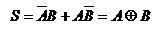 ………… equation (1a).
 ……………..... equation (1b).
Logic Circuit of and
Half Adder:

Figure 1a: Half Adder Logic circuit

Figure 1b: Block Diagram of Half adder
//-------------------------------------------------------------------------
//Verilog Hardware Description Language
(HDL) code for Half Adder
//Structural
model of Module_1 (Half adder) with Verilog HDL
module H_Adder (S, C,
A, B);
input A, B;
output C,
S;
xor (S, A, B);
and (C, A, B);
endmodule
//-------------------------------------------------------------------------
//-----------------------------------------------------------------------
// Test
bench for H_Adder
module t_H_Adder;
wire C, S;
reg
A, B;
H_Adder H_A1 (S, C, A, B); // Instance
name required
initial
begin
A =
1'b0; B = 1'b0;
#100 A = 1'b0; B = 1'b0;
#100 A = 1'b0; B = 1'b1;
#100 A = 1'b1; B = 1'b0;
#100 A = 1'b1; B = 1'b1;
end
initial #500 $finish;
endmodule
//------------------------------------------------------------------------

Figure 2: Simulation output for Half adder Verilog HDL in ModelSim


Carry:


Substituting for half adder equations in that of Full adder, let’s denote Sum of half adder by SH and Carry for Half adder asCH. We can deduce that;


Figure 3b: Full adder implementation with two Half adder circuits

Figure 3c: Full adder block diagram

Figure 4: Full adder HDL Simulation with ModelSim
FOUR-BIT BINARY ADDER


Figure 4b: Four-bit adder block diagram
//-----------------------------------------------------


If we study figure 7 critically with figure 6, we will notice that Pi and Gi are the Sum and Carry output of the first half adder in the module while (Pi exor Gi) is the Sum of the whole Full adder module. In the design of a four-bit binary adder employing the carry lookahead generator, in this circuit, our C1, C2, C3 (carry output from adder 1, 3, and 3 respectively) are available immediately we have the four bit augend A0A1A2A3 and the addend B0B1B2B3 with the initial carry-in to the Lowest Significant Binary (LSB) and thus reduce the carry propagation delay time figure 8, bellow.


Figure 11: Four-bit binary Adder/Subtractor

FULL ADDER CIRCUIT
DESIGN
A full adder adds binary numbers and
accounts for values carried in as well as out. A one-bit full adder adds three
one-bit numbers, often written as A, B, and
Cin, is a bit carried in
from the next less significant stage. In practical, the full-adder is usually a
component in a cascade of adders, for the addition of 8, 16, 32, etc. bits
binary numbers. The circuit produces a two-bit output, output carry and sum
typically represented by the signals Cout and S. The truth table for a 1-bit full adder is
described in table 2 bellow.
Table 2: Truth
Table for 1-bit Full adder
A
|
B
|
Cin
|
S
|
Cout
|
0
|
0
|
0
|
0
|
0
|
0
|
0
|
1
|
1
|
0
|
0
|
1
|
0
|
1
|
0
|
0
|
1
|
1
|
0
|
1
|
1
|
0
|
0
|
1
|
0
|
1
|
0
|
1
|
0
|
1
|
1
|
1
|
0
|
0
|
1
|
1
|
1
|
1
|
1
|
1
|
Simplification Using K-Map:
Sum:
Carry:
Substituting for half adder equations in that of Full adder, let’s denote Sum of half adder by SH and Carry for Half adder as
Figure 3: Full adder Logic circuit
Figure 3b: Full adder implementation with two Half adder circuits
Figure 3c: Full adder block diagram
//--------------------------------------------------------------------
//Full adder verilog HDL Code using the half
adder instance
module
F_Adder (S, Cout, A, B, Cin);
output
S,Cout;
input
A, B, Cin;
wire
S1, C1, C2;
H_Adder HA1 (S1, C1, A, B);
H_Adder HA2 (S, C2, Cin, S1);
or
(Cout, C1, C2);
endmodule
//--------------------------------------------------------------------
//--------------------------------------------------------------------
// Test bench for F_Adder
module
t_F_Adder;
wire S,
Cout;
reg A, B, Cin;
F_Adder
F_A1 (S, Cout, A, B, Cin); // Instance name required
initial
begin
A =
1'b0; B = 1'b0; Cin=1'b0;
#100 A =
1'b0; B = 1'b0; Cin = 1'b0;
#100 A =
1'b0; B = 1'b0; Cin = 1'b1;
#100 A =
1'b0; B = 1'b1; Cin = 1'b0;
#100 A =
1'b0; B = 1'b1; Cin = 1'b1;
#100 A =
1'b1; B = 1'b0; Cin = 1'b0;
#100 A =
1'b1; B = 1'b0; Cin = 1'b1;
#100 A =
1'b1; B = 1'b1; Cin = 1'b0;
#100 A =
1'b1; B = 1'b1; Cin = 1'b1;
end
initial
#900 $finish;
Figure 4: Full adder HDL Simulation with ModelSim
FOUR-BIT BINARY ADDER
Given a 4-bit binary augend A3 A2 A1 A0 and the addend B3
B2 B1 B0. We can perform binary addition A+B
using a cascade of adders shown in figure 4, bellow;
Figure 4: Four-bit adder design
Figure 4b: Four-bit adder block diagram
//-----------------------------------------------------
//Verilog HDL Code for 4-bit adder
module
four_bit_adder(S, C4, A, B, C0);
input
[3:0] A, B;
input C0;
output [3:0] S;
output C4;
wire C1,
C2, C3;
//four
bit adder body from instance of full_adder
F_Adder F_A1 (S[0], C1, A[0], B[0], C0);
F_Adder F_A2 (S[1], C2, A[1], B[1], C1);
F_Adder F_A3 (S[2], C3, A[2], B[2], C2);
F_Adder F_A4 (S[3], C4, A[3], B[3], C3);
endmodule
//----------------------------------------------------------
//--------------------------------------------------------------
// Test bench for 4_bit_Adder
module t_four_bit_adder;
wire
[3:0] S;
wire C4;
reg [3:0]A, B;
reg C0;
four_bit_adder
F1(S, C4, A, B, C0);
initial
begin
A[3:0] = 4'b0000; B = 4'b0000; C0 = 1'b0;
#100
A[3:0] = 4'b1010; B = 4'b1001; C0 = 1'b0;
#100
A[3:0] = 4'b0010; B = 4'b1001; C0 = 1'b1;
end
initial
#300 $finish;
endmodule
//--------------------------------------------
Figure 5: Four-bit adder simulation
CARRY LOOKAHEAD LOGIC
CIRCUIT DESIGN
In the four-bit circuit design above, the output of the
adder cannot be completely determined until the carry propagates through the
full adders. Carry lookahead logic,
is the technology that is widely used to reduce the propagation time of adder
circuits and make their arithmetic operations faster.
Figure 6: Full adder circuit showing P and G signals
In the circuit of described in figure 5, “the signals at Pi and Gi
settle to their steady-state values after they propagate through their
respective gates”, (Mano, 2013). The two signals are common to half adders and
depend on only the input augend and addend bits, (Mano, 2013).
The carry propagation time is a
very important attribute of an adder as it determines the speed at which it
adds two numbers, (Mano, 2013). All other arithmetic operation in digital
system can be performed by successive additions, this makes the time take
required for addition process critical to digital arithmetic operations. By
trading complexity of equipments for
speed, we use the carry lookahead logic for
reducing the carry propagation time in a parallel adder as described bellow.
Considering the circuit in figure 6;
The output sum and carry can respectively be expressed as:
From equation (4), we
can deduce that if;
C0 = input
carry
With the equations above, we can deduce that not minding the cost and complexity of
the circuit, we may not need to wait for the carries (C1,C2,C3) to propagate through the circuit before getting
the result of our addition. Figure 7
bellow shows the logic circuit diagram for the carry lookahead generator.
Figure 7: Carry lookahead Generator
//---------------------------------------------------------------------
//Carry lookahead generator model with
Verilog HDL
module Carry_lookahead_gen (C1,C2,C3, P0, P1, P2, G0, G1, G2, C0);
input P0, P1, P2, G0, G1, G2, C0;
output
C1,C2,C3;
wire w1,
w2, w3, w4, w5, w6;
and (w1, P0, C0);
or (C1, w1, G0);
and (w2, P1, G0);
and (w3, P0, P1, C0);
or (C2, w2, w3, G1);
and (w4, P2, G1);
and (w5, P1, P2, G0);
and (w6,
P0, P1, P2, C0);
or (C3, w4, w5, w6);
endmodule
//-------------------------------------------------------------------------
If we study figure 7 critically with figure 6, we will notice that Pi and Gi are the Sum and Carry output of the first half adder in the module while (Pi exor Gi) is the Sum of the whole Full adder module. In the design of a four-bit binary adder employing the carry lookahead generator, in this circuit, our C1, C2, C3 (carry output from adder 1, 3, and 3 respectively) are available immediately we have the four bit augend A0A1A2A3 and the addend B0B1B2B3 with the initial carry-in to the Lowest Significant Binary (LSB) and thus reduce the carry propagation delay time figure 8, bellow.
Figure 8: Four-bit
adder with carry lookahead generator
Figure 9: Signal
waveform for 4 bits adder with carry lookahead generator from ModelSim
simulation for the first 100ns.
In figure 9, the first change of bits at 100ns depicted by
the yellow line, C4 = 1, S3,S2,S1,S0 = 0011,
A3A2A1A0 = 1010, B3B2B1B0
= 1001, and C0 = 0
Figure 10: Signal
waveform for 4 bits adder with carry lookahead generator from ModelSim
simulation for the second 100ns.
FOUR-BIT BINARY ADDER/SUBTRACTOR
We can perform subtraction of unsigned numbers conveniently
by means of 2’s complements. A-B = A+(-B) and –B = 2’s complement of B. The 2’s
complement can be obtained by taking the 1’s complement and adding 1 to the
least significant pair of bits.
The circuit described in figure 11 bellow is designed to perform addition and subtraction of
four-bit binary in two’s complement.Figure 11: Four-bit binary Adder/Subtractor
In the circuit the augend bit
i.e. A0A1A2A3 is added to the
addend bit B0B1B2B3 when the
circuit is performing addition, M = 0, and when it is to perform subtraction
M=1. When M=0 meaning, the circuit is to perform arithmetic A3A2A1A0
+ B3B2B1B0, when M=1 then the
operation is A3A2A1A0 – B3B2B1B0
in the latter case, the circuit actually perform A3A2A1A0
+ (-B3B2B1B0), (-B3B2B1B0)
is given by 2’complement of - B3B2B1B0.
In this case, since M=1, the
output of the Exclusive-Or gates in the circuit will be 1’complement of B3B2B1B0,
the addition of C0 which is now ‘1’ makes the result the two’s complement
of B3B2B1B0.
The output of the circuit will be S3S2S1S0,
this is the correct answer. In the case of signed binary number, there are some
things to be noted, firstly, the Most Significant Binary (MSB) indicates the
sign of the binary number 1=> negative, 0=> Positive, and also the output
V in the figure 11, if V=0, then there is an overflow, an overflow indicates
that the result of the addition or subtraction is beyond the range of representation
of the number of binary bits.
It is worth to note at this point that signed binary
number of n bit can represent number
ranges from -2n-1 to 2n-1-1. There is need for some
little enhancement of circuit in figure 11, to enable
it display correct result for signed binary numbers. It’s waveform output for
simple addition and subtraction is given in figures 12 and 13 bellow.
//------------------------------------------------------------------------
// Verilog Code for adder/ subtraction circuit
in figure 11
module
add_sub(S,V, A, B1, M);
input
[3:0] A, B1;
input M;
output [3:0] S;
output V;
wire [3:0]B;
wire C1,
C2, C3;
//four
bit adder body from instance of full_adder
F_Adder F_A1 (S[0], C1, A[0], B[0], M);
F_Adder F_A2 (S[1], C2, A[1], B[1], C1);
F_Adder F_A3 (S[2], C3, A[2], B[2], C2);
F_Adder F_A4 (S[3], C4, A[3], B[3], C3);
xor
(B[0], M, B1[0]);
xor
(B[1], M, B1[1]);
xor
(B[2], M, B1[2]);
xor
(B[3], M, B1[3]);
xor (V,
C4,C3);
endmodule
//-----------------------------------------------------------------------
//------------------------------------------------------------------------
// Test bench for adder/subtraction circuit
module
t_add_sub;
wire
[3:0] S;
wire V;
reg [3:0]A, B1;
reg M;
add_sub
a_s1 (S,V, A, B1, M);
initial
begin
A[3:0] = 4'b0000; B1 = 4'b0000; M = 1'b0;
#100
A[3:0] = 4'b1010; B1 = 4'b0001; M = 1'b0;
#100
A[3:0] = 4'b1010; B1 = 4'b0001; M = 1'b1;
end
initial
#300 $finish;
endmodule
//-------------------------------------------------------------------------
Reference
Adder (electronics); “From
Wikipedia, the free encyclopedia”, LINK
Mano M. Morris and
Ciletti D. Michael; “Digital Design With and Introduction to the Verilog
HDL – Fifth Edition” Copyright © 2013, 2007, 2002, 1991, 1984 Person Education,
Inc., publishing as Prentice Hall, One Lake Street, Upper Saddle River, New
Jersey 07458.
Marcus Lloyde George
and Lucien Ngalamou; “A Methodology for Effectively Teaching Digital Design
to Electrical and Computer Engineering Students of the University of the West
Indies (UWI) in Nine Weeks”, Transactions on Eduction.
Peter J. Ashenden (2004); “VHDL
Tutorial”, EDA Consultant, Ashenden
Designs PTY. LTD. www.ashenden.com.au
© 2004 by Elsevier Science (USA).
Samir Palnitkar (1996); “Verilog HDL, A guide to Digital Design and
Synthesis” SunSoft Press 1996.
Valentino Crespi, Aram
Galstyan, Kristina Lerman(3005); “Comparative Analysis of Top-Down and
Bottom-up Methodologies for Multi-Agent System Design”, AAMAS’05, July 25-29, 2005, Utrecht ,
Nertherlands. Copyright 2005 ACM 1-59593-094-9/05/0007…$5.00.
No comments:
Post a Comment
Please drop your comment here, thanks.