Computers understand binary number system while humans are
used to arithmetic operations in decimal number systems. To enhance
Computer-Human relationship in this perspective, arithmetic operations are
performed by the computer in a binary
coded decimal, (BCD) form.
In this article I’ll analyse and design a BCD adder which
requires a minimum of nine inputs and five outputs, four bits are require to
code the aguend and the addend making eight bits, and the circuit input carry
makes the nine inputs. The four bit sum output and the output carry represents
the five outputs.
Consider adding 9+9+1 in decimal, the result is 19, in
straight binary this should produce an output 100112, this is an
invalid number in BCD, because in BCD code the group of four bit binary only
represent decimal numbers 0-9. The table bellow shows decimal numbers 0-19 with
their corresponding binary and BCD codes. The K and C in the table are the
respective binary carry and BCD carry bits.

Bellow the ruled level on the table, the BCD adder should detect
that the binary codes are unusable in BCD coding system and provide the
necessary correction. The conditions for the levels on the table where
correction is required a;
- Point where binary sum has output carry K =1 or,
- where Z8 and Z2 are both = 1 or,
- where Z8 and Z4 are both = 1.
The gives the expression for correction requirement: Cor = K + Z8Z4
+Z8Z2
When Cor = 1, it is necessary to add 0110 to the binary sum
and provide an output carry for the next stage.
For example:
Adding:


Figure 1: Block diagram of BCD adder
When an output carry K
= 0 nothing happens as the out S8S4S2S1 is added to 0000 in the second
4-bit adder, but when K=1 OR Z8&Z4 OR Z8&Z2 is equal to ‘1’, the output carry generates a ‘1’, thus “0110”
is added to the output of the first 4-bit adder. The MSB 0 and LSB 0 in the
“0110” to be added is generate by the EXOR gate which accept the output carry
at its two input, either the output carry is 0 or 1 the EXOR generates a ‘0’
(both its input are equal).
The CBCD is the carry generated by the BCD adder,
whenever the output of the OR-gate is ‘1’ a carry is generated by the BCD adder
to the next four-bit group of the BCD code, carry output generated by the 4-bit adder of the second stage is discarded as it will provided by CBCD as required. Bellow is the Verilog HDL code for
BCD adder and figure 2,3, and four shows the simulations changing the bits
value at 100ns, 200ns and 300ns.
//-----------------------------------------------------
module BCD_adder(S, C,
A, B, C0);
input [3:0] A, B;
input C0;
output [3:0] S;
output C;
wire C1, C2, C3, C4,
C5;
wire [3:0]X, Z;
and (C1, Z[3], Z[2]);
and (C2, Z[3], Z[1]);
or (C, C3, C1,C2);
xor (C5, C, C);
assign X[2] = C;
assign X[1] = C;
assign X[3] = C5;
assign X[0] = C5;
//four bit adder body
from instance of full_adder
four_bit_adder F_1 (Z,
C3, A, B, C0);
four_bit_adder F_2 (S,
C4, X, Z, C0);
endmodule
//----------------------------------------------------------//-------------------------------------------------------------
// Test bench for
BCD_Adder
module t_BCD_adder;
wire [3:0] S;
wire C;
reg [3:0]A, B;
reg C0;
BCD_adder F1(S, C, A,
B, C0);
initial
begin
A[3:0] = 4'b0000; B = 4'b0000; C0 = 1'b0;
#100 A[3:0] = 4'b1001;
B = 4'b1001; C0 = 1'b0;
#100 A[3:0] = 4'b1000;
B = 4'b0011; C0 = 1'b0;
#100 A[3:0] = 4'b0100;
B = 4'b0011; C0 = 1'b0;
end
initial #400 $finish;
endmodule
//--------------------------------------------
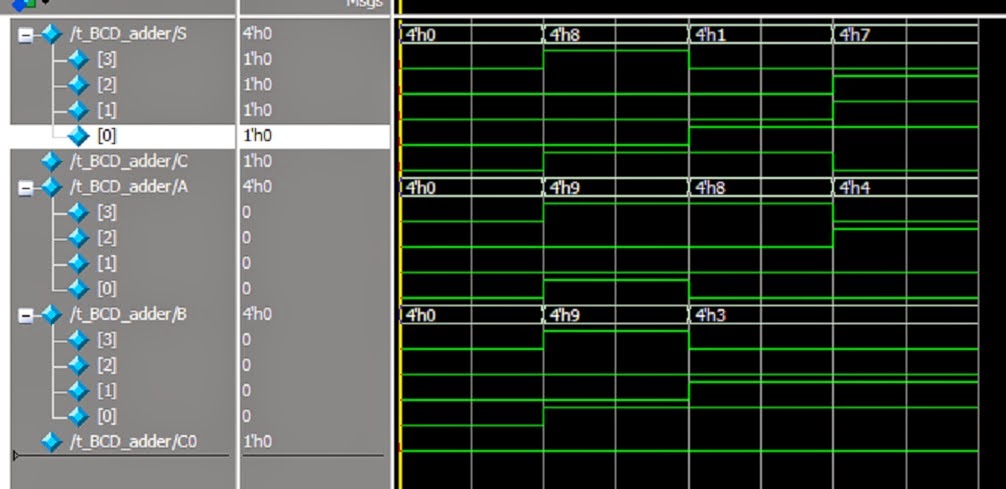
Figure 2: Simulation showing the initial bits value of A: 0000, B: 0000, Sum S: 0000 and Carry C: 0 for the BCD adder (i.e. 0 + 0 = 0 0).

Figure 3: Simulation showing the bits value at 100ns for A: 1001, B: 1001, Sum S: 1000 and Carry C: 1 for the BCD adder (i.e. 9 + 9 = 1 8 ).

Figure 4: Simulation showing the bits value at 300ns for A: 1000, B: 0011, Sum S: 0001 and Carry C: 1 for the BCD adder (i.e. 8+ 3 = 1 1 ).

Figure 5:
Simulation showing the bits value at 300ns for
A: 0100, B: 0011, Sum S: 0111 and Carry C: 0 for the BCD adder (i.e. 4+
3 = 0 7 ).
Reference
Mano M. Morris and
Ciletti D. Michael; “Digital Design With and Introduction to the Verilog
HDL – Fifth Edition” Copyright © 2013, 2007, 2002, 1991, 1984 Person Education,
Inc., publishing as Prentice Hall, One Lake Street, Upper Saddle River, New
Jersey 07458.
|
No comments:
Post a Comment
Please drop your comment here, thanks.